In order to setup your environment to run Cadence applications you need to open a terminal window and type:
. cadence2009
cd cadence
cd tutorial
ln -s var/home/hplp/osuflow/osu_stdcells/lib/tsmc018/lib .
mkdir encounter
cd encounter
For this tutorial you will need a few extra files, all the results of the previous tutorials, make sure you have those.
From the encounter directory type:
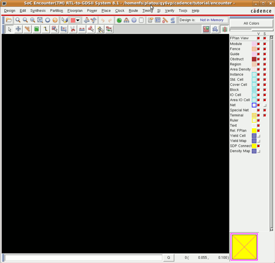
encounter
The window has three main areas:
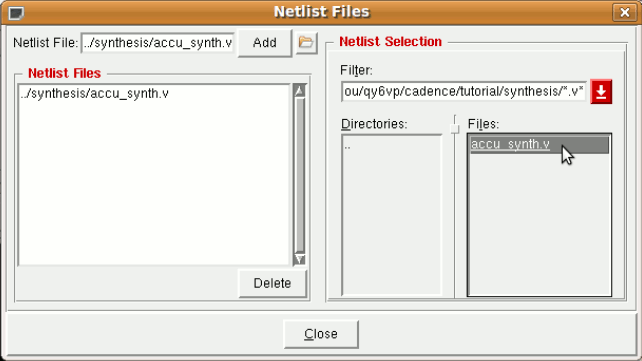
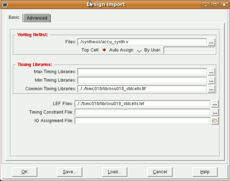
Now we can start using Encounter. First we need to import the synthesized netlist (the result of RTL synthesis with RTL Compiler). Click on Design -> Import Design and the Design Import window should pop-up (as an aside, it seems you can also import RTL directly, I assume this means you can do RTL synthesis in Encounter directly without using RC, it would be interesting to try this and see how it works). Now you need to fill in the Verilog netlist (use the browser button on the right to navigate to your synthesized netlist, in my case accu_synth.v in ../synthesis, make sure you click on Add, then on Close
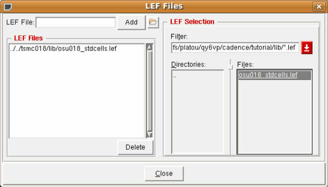
Then click on Auto Assign for the Top Cell assignment. Then we need to specify the physical definitions for the library, do that by clicking on the navigate button on the right of the LEF Files entry which should pop-up the LEF Files window. Navigate to the lib directory (that you just linked into your tutorial directory, in my case at ../lib) then click on osu018_stdcells.lef, and finally on Add, then on Close
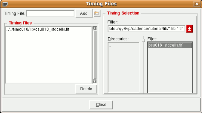
Then we need to specify the timing definitions for the library, do that by clicking on the navigate button on the right of the Common Timing Libraries entry which should pop-up the Timing Files window (note that more advanced libraries will have Max Timing and Min Timing Libraries in order to be able to do "corner analysis", not just nominal analysis). Navigate to the lib directory (that you just linked into your tutorial directory, in my case at ../lib) then click on osu018_stdcells.tlf, and finally on Add, then on Close
Normally, if this was a full chip design, we would also have to specify the I/O pad information now by the IO Assignment File, but for now we will not use I/O pads. Your Design Import pop-up window should look like this now
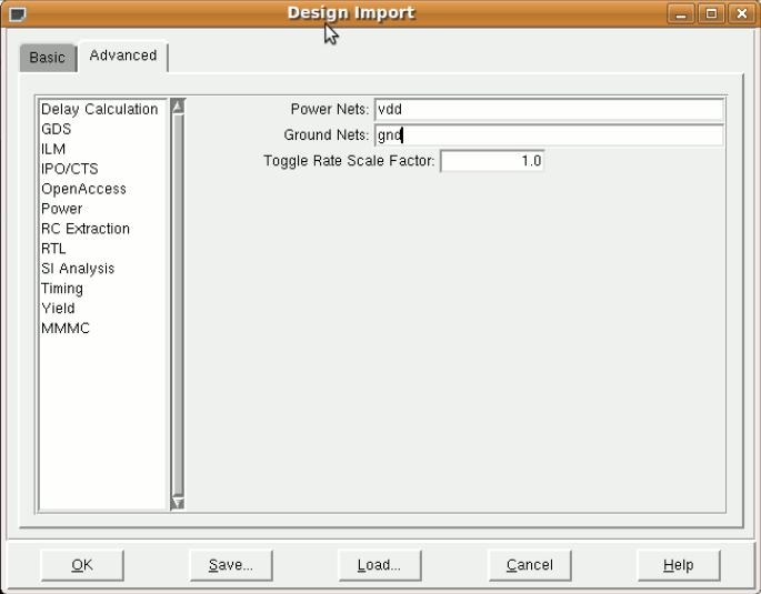
Now click on the Advanced tab and choose Power from the left window, fill vdd for Power Nets and gnd for Ground Nets (out of curiosity you can check that indeed these are the names of the power and gnd nets in your Verilog netlist by opening the file in a text editor).
((Now click on the IPO/CTS tab and fill buf for Buffer Name/Footprint and inv for Inverter Name/Footprint (out of curiosity you can check that indeed these are the footprint names by examining the .tlf file in the lib directory). Also click on Generate Footprint Based on Functional Equivalence.))

Finally click on OK in your Design Import pop-up window. Get familiar with some of the widgets, for example the Design Browser widget (the 7th from the right, top row) lets you see the design hierarchy, etc.
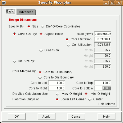
Now we need to specify floorplaning information. Since our design is simple and flat there is not much that needs to be done, but in general now is the time to decide how the big blocks that make up the design should be placed with respect to each other. Click on Floorplan -> Specify Floorplan and leave all defaults except change to 100.00 (default is 0.00) the Core to Left, Core to Right, Core to Top and Core to Bottom.
Click on Apply and the floorplan should change to reflect the 100 micron periphery around the core.
Now you can also play with the aspect ratio on the Specify floorplan window, change that to 0.5, click Apply, then to 2, click Apply again, finally back to 1 and click Apply. Note how the number of rows in your floorplan changes from 5 (for 1) to 7 (for 2) to 3 (for 0.5). It is a good idea to save your design from time to time by Design -> Save Design As...
The next step is to create the power and ground connections, but first you have to specify the nets. Click on Floorplan -> Connect Global Nets and then fill the pop-up window connecting pin vdd to global net vdd, and pin gnd to global net gnd, making sure the button Apply All is checked (need to do this one at a time by adding to list). Click Apply, then Check (make sure there are no warnings here), then Close to close the pop-up.

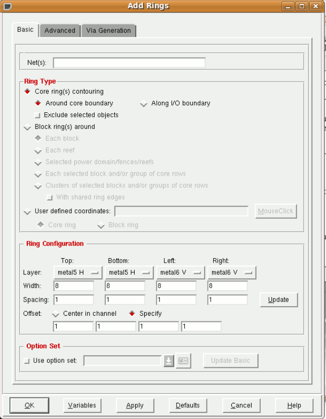
Now we can finally create the power distribution for our design. Click Power -> Power Planning -> Add Rings. Choose metal 5 and metal 6 with the width and spacing of 8 and 1 and with offset of 1, then click Apply, followed by Cancel.
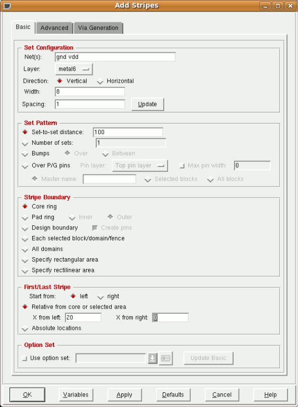
Click Power -> Power Planning -> Add Stripes. Choose metal 6 with the width and spacing of 8 and 1 and with X from left of 20, then click Apply, followed by Cancel.
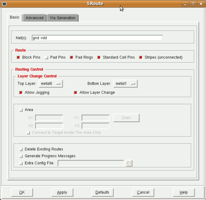
Then, in order to route the rest of the power distribution click Route -> Special Route, deselect Pad pins, then click Apply, followed by Cancel.
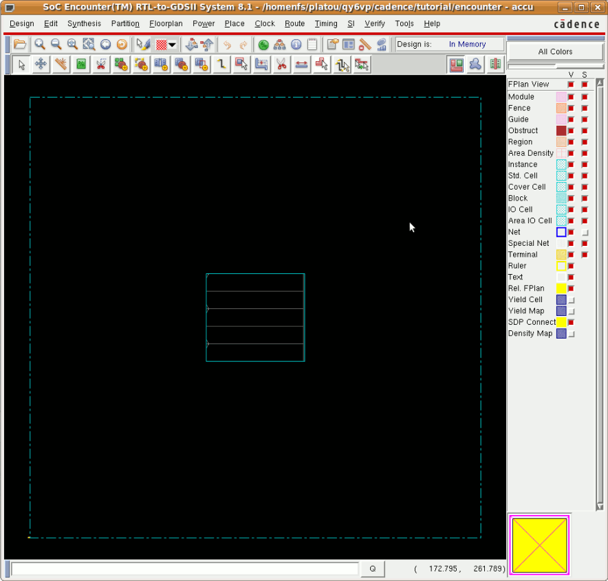
Now your floorplan should look like this.

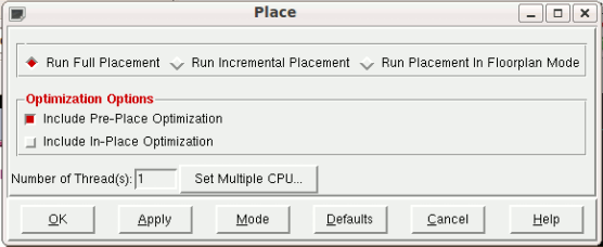
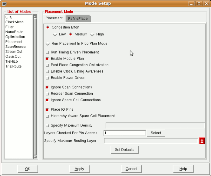
It is time to place our cells, go to Place -> Standard Cells, click Mode, then deselect Run Timing Driven Placement and Reorder Scan Connection then click Apply, followed by Cancel.
Now, if you click on the Physical View widget (on the right of the second row of the widget menu, right to the left of All Colors) you will see your placed design.

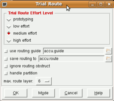
Finally we can also route our design, go to Route -> Trial Route... and click OK
And now your design should be also routed.
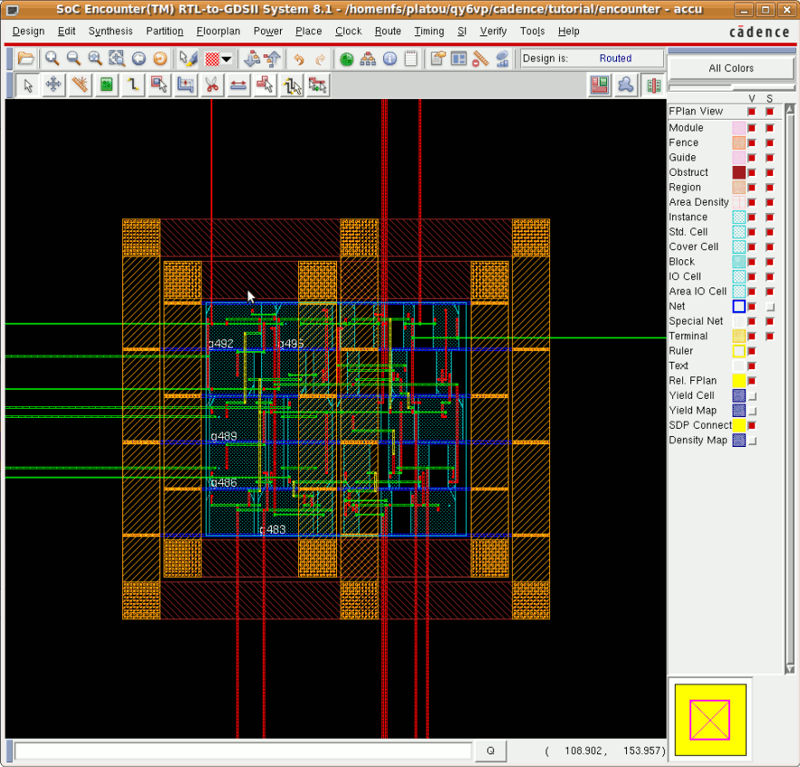
Since we don't have pads in our design the tools route the primary inputs and outputs to the periphery of the floorplan such that they can in principle be connected in a hierarchical fashion to other blocks.
Congratulations, this is the end of the first Backend Tutorial, in future tutorials you will learn how to do clock tree synthesis, verify your design, power analysis, timing analysis, and signal integrity.