
. cdscdk2003 cd cadence icfb &
For more information on the various Cadence tools I encourage you again to read the corresponding user manuals.
The Tutorial library that you created previously should still appear in the Library Manager window. You can still use the same library for now. Before we start we need to add three more (existing) libraries to our Library Manager. Go to Tools -> Library Path Editor in the CIW. Add the following 3 libraries:
analogLib basic sample
with paths:
$CDS/ic/tools/dfII/etc/cdslib/artist/analogLib $CDS/ic/tools/dfII/etc/cdslib/basic $CDS/ic/tools/dfII/samples/cdslib/sample
Your Library Path Editor window should look like this:
Now click on File -> Save , then Exit in the Library Path Editor window. Let's start our third schematic!
From this dialog window you can create a default inverter symbol. The only disadvantage with this method is that the default shape is a box and you would need to change that (no big effort really). So for now press Cancel and let's try a different method, remembering that you can always create a symbol from scratch in this way.
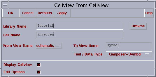
Since the inverter is a very common gate it is likely that a symbol with the desired shape already exists and we can use it without having to explicitely create the symbol from scratch. For example the sample library in the Library Manager window has a generic inverter cell, go to this library and click on the symbol view of the inv cell.

Now do Edit -> Copy and let the From entries unchanged but fill the To entries with the symbol view of your inverter schematic in the Tutorial Library.
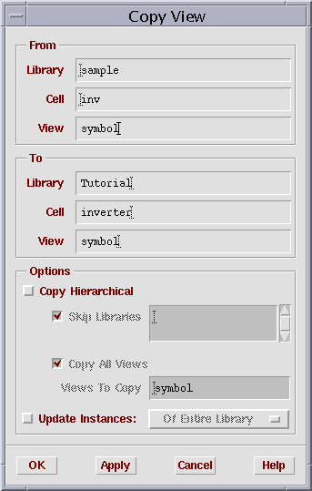
Press OK. You may get a Copy Problems window pop-up, just press OK, it's really just a warning. p> If you go now to your Tutorial library to the inverter cell you should find that it now has two views, schematic and symbol. Open both the schematic view and the symbol view by double clicking on the schematic and the symbol view in the Library Manager window. You can notice that the input and output ports have different names (IN and OUT in our schematic, but A and Y in the symbol). We need to edit the symbol to change the two port names such that they match with the names in the schematic. Go to Edit -> Properties -> Objects in the Symbol Editing window and then click on the small square representing the input pin. Change A to IN and Display from off to value.
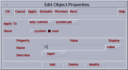
Click OK. Similarly change Y to OUT. Now notice that there are still the two labels A and Y that need to be deleted on the Symbol.
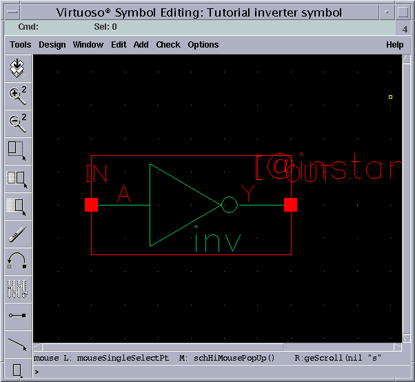
Delete them by clicking on the Delete button on the left (looks like a pencil) or by doing Edit -> Delete and then click on the lables (A and Y). Then you can click and drag the IN and OUT pin values to more convenient locations. You should get something like this.

Now you need to save your symbol (click on the left Save button or do Design -> Save, and then go to the Schematic window and do Check and Save. You should get no errors or warnings, if you get any errors you need to go back and fix them. Close the inverter schematic and symbol windows.

Now click once to place the left most inverter, then move the mouse to the right and click again to place the remaining ones. If you make a mistake you can always do Edit -> Undo and try again.

Press ESC. Now we need to place the other remaining 5 inverters but they need to face left. For this we do again place instance with 1 Row and 5 Columns but before we place the inverters we need to click twice on the right mouse button, this will rotate the inverter symbol by 180 degrees. Then click the left mouse button once for the right most inverter, then move the mouse to the left and place the remaining inverters. Don't be afraid if you make mistakes, just Undo and start over.
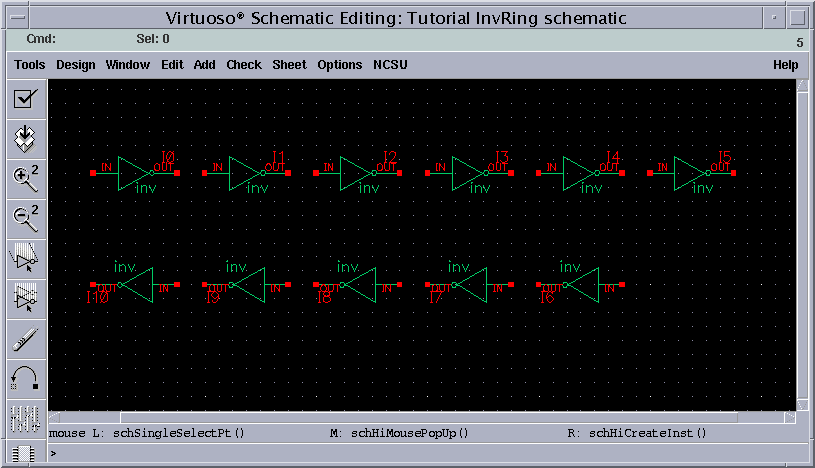
Now we only need to wire the 11 inverters into a ring and add a vdd and a gnd symbol from the NCSU_Analog_Parts -> Supply Nets library (leave them unconnected on the top). Do Check and Save and make sure you have no errors or warnings.

The schematic of the inverter should now appear in the schematic window. Now you can edit the inverter (if you want), then check and save. This will change all inverter instances in your hierarchical schematic. We don't really need to make any changes now, but you will have to make changes for your homework. For now let's just go back up by doing Design -> Hierarchy -> Return. You should now have your InvRing schematic back up.
As in Tutorials 1 and 2 we first need to set up the right simulator (spectre), then set the two model library files for the nmos and pmos (please revisit Tutorial 1 for the details). We also need to set up the power supply. Go to Setup -> Stimuli. In general you have to set up Inputs and Global Sources, but in this case we don't have any explicit inputs. We only need to setup the global sources (power supply) since there are no other inputs or outputs for the ring oscillator. Click on the Global Sources, you should have only one (vdd!). Click on Enabled, Function dc, Type Voltage, DC voltage 5, Source type dc, and click on Apply. The vdd! should turn from OFF to ON. Click OK. CAUTION Cadence is very fragile concerning this dialog box, make sure you enter the numbers exactly as above (i.e. no space between the digit and n, etc.). If you get syntax errors later in simulation they are most likely because of this. Now you need to choose the type of simulation, go to Analyses -> Choose... In this case we will choose tran which is the default, 4n as the Stop time and moderate as the accuracy default. Now go to Outputs -> Save All and make sure allpub is checked for signals to save (default). Click OK. CAUTION In general, once you have a big schematic, you will want to only save a few signals for simulation, this will make your simulation faster. For small circuits as we have now it doesn't make a big difference though.
In order to help with convergence we can also set up some initial conditions, for example make the left-most node a zero. Go to Simulation -> Convergence Aids -> Initial Condition then click on the left most node in the schematic. A big zero should appear on top of the net. Click OK.
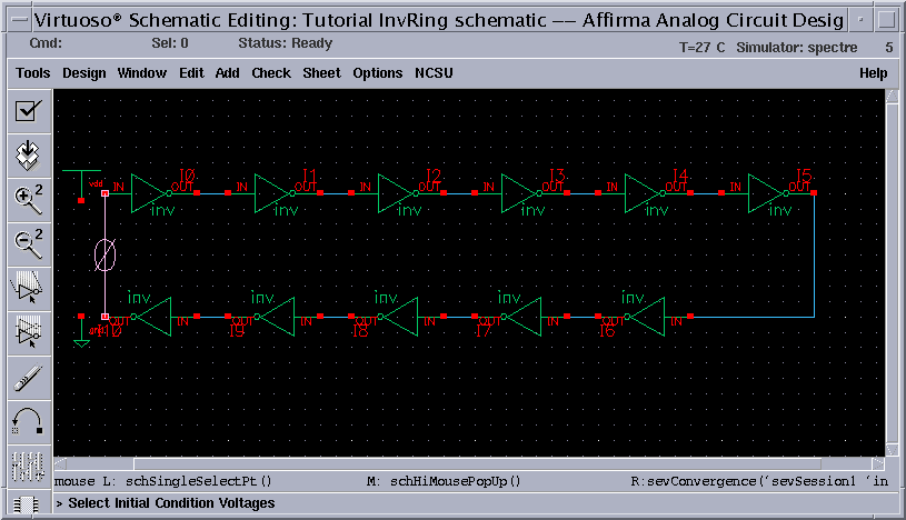
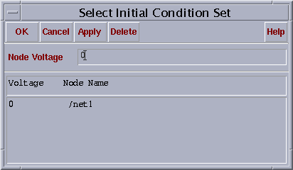
Also the net should appear in the Select Initial Condition dialog box.
Now we can finally simulate! Click on the Netlist and Run button (looks like a green light) on the right or go to Simulation -> Netlist and Run. Click OK on the Welcome to Spectre window which should start the simulation. In case you have errors you will need to go back and correct them. This can be tricky! You may need to do Simulation -> Netlist -> Recreate if you change the schematic. CAUTION Each time you change the schematic you have to do Check and Save!. Assuming there are no errors you can now admire the simulation results. Go to Results -> Direct Plot -> Transient Signal which will pop-up your schematic window. Now you have to click on the signals you want to see. Since this is a transient analysis we want to see a few voltages. In order to do this you have to click on the desired nets, then the ESC key (try not to choose the signal with the initial condition of 0 since the transient there may be worse than on the other inverters). You should finally get the desired simulation results, some glorious periodic signals as expected from an ring oscillator. You can determine the period of oscillation, measure the inverter delay and compare that with what we learned in class.

Now we can measure tpLH, tpHL for the second and third inverters. To do this accurately we are going to use the waveform calculator. Go to Tools -> Calculator in the Analog Environment window which should pop up the calculator. Get familiarized with the calculator, you may also want to consult Help or cdsdoc. The calculator works with a "stack" (like some HP calculators) in which you first input one or more operands (waveforms) and then you perform an operation on them. After each operation it's recommended that you clear the stack (clst). To view the stack you have to enable it (click on the button Display Stack on top). Now click on wave in the calculator window and then click on the latest wave in the waveform window (goes from low to high first). A wave name should appear in the calculator window. Now press on the earlier wave of different polarity (goes from high to low first) which should push the first wave in the stack and bring this new wave in the calculator. IMPORTANT: Note that we entered the waves in reverse order (the late first, then the early one), this is a "feature" of the stack operation of the calculator.

Now go to Special Functions -> delay in the calculator window (top). Fill 2.5 as the threshold values (50% of Vdd = 5V) and keep the edges as 1 and edge types as either (in other situations you may want to make different choices here) then click OK.

Notice the change in the calculator window. Now click on Evaluate buffer and you should get the value of tpLH for the inverter with the latest waveform as an output. Clear Evaluate buffer and clear the stack (clst) and now measure tpHL for the second inverter. You need to go through the same steps except choose Edge Number 2 in the Threshold Delay dialogue box. You can also see the waveforms independently, not all 4 on the same graph. In the Waveform Window just got to Axes -> To Strip, and the waveforms will be independently displayed.
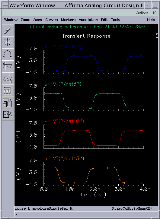
You can always go back to displaying all waveforms on the same graph by doing Axes -> To Composite. It is a good idea to save your state before exiting the simulator in case you want to redo some of the simulations you can start by loading a saved state. Congratulations, this is the end of Tutorial 3.