
Click Apply, then change the names to get all 4 cells, then click Cancel to close the pop-up window.
Open the schematic view of Invx1 by double clicking on the schematic view in the Library Manager window. We now need to change the properties Width and Length for the transistors such that they are parameterized. Edit properties for the nmos and change Length to: Len and Width to: Wid, then pmos and change Length to: Len and Width to: a*Wid.

Check and save your design and make sure you get no errors. By doing this we have created parameterized transistor sizes where both the nmos and pmos have the same length with parameter Len (default value 0.6u), while the widths are parameters Wid and a*Wid where a can be used to change the PMOS/NMOS ratio and Wid is the base size (e.g. 1.5u). When we use this inverter in a hierarchical schematic we can now keep the default values or change the default values to go to a different technology (e.g. change Len to 0.25u for a 0.25u CMOS technology) or have different transistor strengths for different inverters.
Now change the sizes for Invx4, Invx16 and Loadx64. For all of them make the length Len, both for PMOS and NMOS. This is the standard practice for digital design where transistors are minimum length for high performance. Then make the widths:
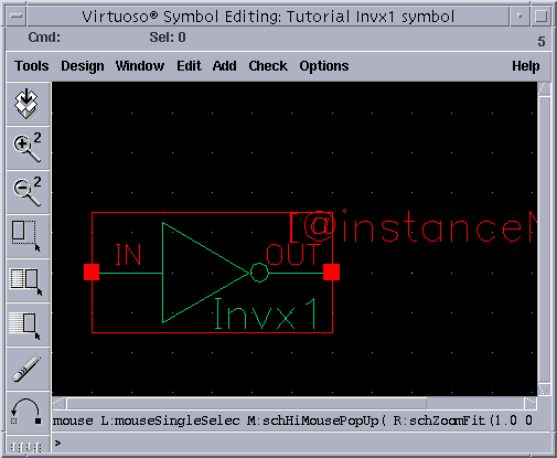
We should also edit the symbols of the 4 new cells to reflect their different characteristics, although this is not absolutely necessary. Let's do it though, go to the Library Manager and double click on the symbol view of the Invx1 cell. Go to Edit -> Properties -> Objects... and then clik on the text inv on the symbol itself. In the pop-up window fill Invx1 as the Label, then clik OK. The symbol should change to reflect the change. Make sure you also save the symbol.
Also change the names of the three other new cells to: Invx4, Invx16, Loadx64.
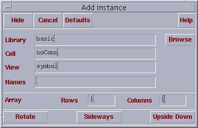
Now we can create a hierarchical schematic that uses the newly created inverter symbols. Let's do that by creating a new schematic, call it InvDelay. Go to the Library Manager and with the Tutorial library highlighted do File -> New -> Cell View and create a schematic view for a cell named InvDelay. The Composer schematic editor window should open up. Let's create a schematic of 4 cascaded inverters with an input port IN1 and an output port OUT after the third inverter, first inverter Invx1, second Invx4, third Invx16, fourth Loadx64. You may need to go to the previous tutorials if you don't remember all the steps. Do Check and Save. You should get one warning about the output of the last inverter which is floating. Let's get rid of that warning by placing an instance of the noConn instance from the basic library on that output.
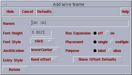
Also add labels to the internal nets by doing Add -> Wire Name, filling the names: IN2 IN3 in the dialogue box and then click on the two internal nets, then on CANCEL.
Now when you do a Check and Save you should get no errors or warnings and the two internal nets should have names.

Now let's assign sizes to the 4 inverters. Let's assume that we are interested in the inverter delay for a fanout of 4; this means that in theory we could use identical inverters and place 3 more of them at each output (we did that in Tutorial 3), or use the newly created parameterized inverters. and assume that an inverter 4 times larger than the base size is equivalent to 4 base inverters (if you are unclear about this please check the text, notes, talk to the TA or come and see me). This means that we can keep the first inverter at the base size, make the second one 4 times larger, the 3rd one 16 times larger and the 4th one 32 times larger, simply by making the parameter b = 4. In case we want to test a different sizing scenario we just need to modify one parameter, b, to a different value. We can do this easily now since we have already defined the parameterized transistor sizes for the inverter. The last skill in the schematic entry for now will be to traverse hierarchy. For this go to Design -> Hierarchy -> Descend Edit and then click on the first inverter and then clik OK. You should get to the inverter schematic where you can verify that the sizes are actually as you would expect. In principle now you could edit this schematic if necessary but for now go back to Design -> Hierarchy -> Return.
CAUTION: In general you should always use this approach when estimating delays through simulation, never drive inputs directly because you may get unrealistic results!
We use two inverters for delay such that we can take both tpLH and tpHL into account without having to do manual addition. First let's make sure the inverters work, let's simulate. In the Composer window go to Tools -> Analog Environment. The design should be set to the right Library, Cell and View. Setup simulation for Spectre, and set the right model libraries. If you have an old state that you saved you can also load that state to save on typing. We also need to set up inputs and power supply since we don't have explicit voltage sources. Go to Setup -> Stimuli. We need to setup both inputs (IN1) and the global sources (power supply). For IN1 use a pulse with amplitude 5 (Voltage 1=0, Voltage 2=5) with 0.4n rise and fall times and 1.6n pulse width and 4n period, make sure you enable it. Click on the Global Sources, you should have only one (vdd!). Click on Enabled, Function dc, Type Voltage, DC voltage 5, Source type dc, and click on Apply. The vdd! should turn from OFF to ON. You may want to revisit Tutorial 2 if you have trouble with this. CAUTION Cadence is very fragile concerning this dialog box, make sure you enter the numbers exactly as above (i.e. no space between the digit and n, etc.). If you get syntax errors later in simulation they are most likely because of this. Now you need to choose the type of simulation, go to Analyses -> Choose... In this case we will choose tran which is the default, 8n as the Stop time and moderate as the accuracy default. Now go to Outputs -> Save All and make sure allpub is checked for signals to save (default). Click OK. CAUTION In general, once you have a big schematic, you will want to only save a few signals for simulation, this will make your simulation faster. For small circuits as we have now it doesn't make a big difference though.
The only other settings that we need are the variables a, b, c, Len and Wid, for now let's set a=2 (the rule of thumb), b=4, c=64, Len=0.6u, Wid=1.5u. Go to Variables -> Edit and then in the dialogue box enter a as Name and 2 as value. Click Add.

The variable a should now appear in the Design Variables list. Do the same for b, c, Wid, Len. All variables should now appear in the Design Variables list.

Now we can finally simulate! Click on the Netlist and Run button (looks like a green light) on the right or go to Simulation -> Netlist and Run. Click OK on the Welcome to Spectre window which should start the simulation. In case you have errors you will need to go back and correct them. This can be tricky! You may need to do Simulation -> Netlist -> Recreate if you change the schematic. CAUTION Each time you change the schematic you have to do Check and Save!. Assuming there are no errors you can now admire the simulation results. Go to Results -> Direct Plot -> Transient Signal which will pop-up your schematic window. Now you have to click on the signals you want to see. Since this is a transient analysis we want to see a few voltages. In order to do this you have to click on the desired nets, then the ESC key. Click on OUT, IN1, IN2 and IN3.
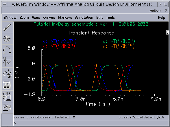
Now we can measure tpLH, tpHL for the second and third inverters (signals IN2 and IN3). To do this accurately we are going to use the waveform calculator. Go to Tools -> Calculator in the Analog Environment window which should pop up the calculator. Get familiarized with the calculator, you may also want to consult cdsdoc. The calculator works with a "stack" in which you first input a waveform or more and then you perform an operation. After each operation it's recommended that you clear the stack (clst). To view the stack you have to enable it (click on the button Display Stack). Now click on wave in the calculator window and then click on the IN3 wave in the waveform window. A wave should be displayed in the calculator. Now press on the IN2 wave which should push the first wave in the stack and bring this new wave in the calculator. IMPORTANT: Note that we entered the waves in reverse order (the late first, then the early one), this is a "feature" of the stack operation of the calculator.

Now go to Special Functions in the calculator window and click on delay. Fill 2.5 as the threshold values (50% of Vdd = 5V) and keep the edges as 1 and edge types as either (in other situations you may want to make different choices here) then click OK. Notice the change in the calculator window. Now click on Evaluate buffer and you should get the value approx. 224 ps which represents tpLH for the second inverter with a fanout of 4 (we measured delay from IN2 to IN3 going high). Clear Evaluate buffer and the stack and now measure tpHL for the second inverter. You need to got through the same steps except choose Edge Number 2 in the Threshold Delay dialogue box. tpHL is about 221 ps, slightly less than tpLH as expected due to the difference in mobility between pmos and nmos. Although this may suggest that we need to increase the size of the pmos even higher we only need to do that if we are mainly interested in symmetric VTC and equal tpHL and tpLH. If we are interested in propagation delay (average of tpHL and tpLH) we may actually want to make them even less symmetric to gain speed. In order to see why we added yet another inverter we can also measure the total delay from IN2 to OUT. For this we again clear the calculator and measure the delay from IN2 and OUT for both the first and the second edge, you should get about 434ps and 433ps, res[ectively. As you can see the two values are very close and also relatively close to the previously measured tpHL + tpLH = 445ps. Basically this means that we can use just one measurement, not two, to get information about tp.
Let's determine now the optimal pmos/nmos ratio a through simulation. For this we will do multiple simulations with different values for a and determine the fastest solution. Theoretically we could do those simulations manually, luckily Cadence offers the possibility of doing this automatically. Go to Tools -> Parametric Analysis in the Analog Environment window. Fill the Variable Name a with values from 1 to 3 in Linear Steps of 0.2

Now do Analysis -> Start in the Parametric Analysis window. The simulations will take a little longer (10 simulations are performed), be patient. Once the simulations are over we can again plot the waveforms. Go to Results -> Direct Plot -> Transient Signal and then choose IN2 and OUT.
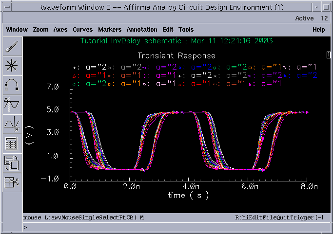
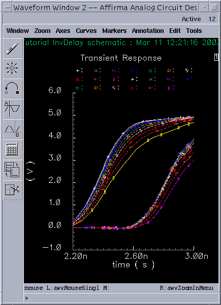
The first observation that we can make is that the delays are quite close even if we changed the pmos/nmos ratio quite drastically (from 1 to 3), which should reinforce the idea that complementary static CMOS is non-ratioed. If we zoom on the HL transition you will discover that the fastest solution in this case is actually the a = 1 waveform where the pmos and nmos are equal (412ps vs. 468ps when a=2.8).

On the other hand if you look at the LH transition you can see that the solution with a = 1 has a poor rise time while a = 1.4 or a = 1.6 have much better rise times and still have small delays (compared to larger or smaller values of a). You should verify that this is indeed true by using the calculator. From this superficial analysis we can conclude that indeed a value around a = 1.5 (close to sqrt(2-3) = 1.41-1.73 as suggested in class) is close to optimal for delay and decent rise time.
It is a good idea to save your state before exiting the simulator in case you want to redo some of the simulations you can start by loading a saved state. Congratulations, this is the end of Tutorial 4.