
. cdscdk2003
. cdscdk
cd Tutorial icfb &
Let's start our fifth tutorial now!
There are several consequences of using the LAMBDA-based rules:
Check and save and make sure you don't have any errors or warnings. If everything looks fine it is finally time to start layout.
Now, whenever you make mistakes you can simply go back with Undo.
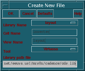
First create a layout view of the inverter cell, go to File -> New -> Cell view and fill in inverter for Cell Name, layout for View Name and Virtuoso for Tool.
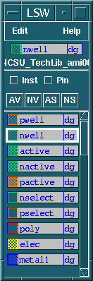
Two windows should pop-up, the Virtuoso layout window screen and the LSW which is used for choosing the layers to be used:
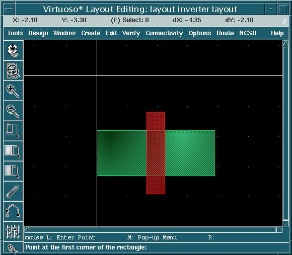
Now get acquainted to the Virtuoso layout screen. It is quite similar to the Composer window, an important addition are the X and Y absolute coordinates and dX and dY relative coordinates on the top, these are very useful for drawing precise dimensions. The numbers are in microns but notice as you move the cursor that the numbers only change as multiples of 0.15u which is the half-LAMBDA value and also the grid spacing. The configuration forces a "snap to grid" policy which is very good for enforcing the SCMOS design rules. All the custom layout is done by drawing rectangles or paths by doing Create -> Rectangle or Create -> Path and chosing the right layer from the LSW window.
Doing a good layout is more than just drawing rectangles though... The most important aspect is planning: you NEED to use a pencil and paper and make a simple sketch of the layout before you start. You need to decide:
First let's do the nmos. We know that the nmos is 5 lambda wide (10 units) which gives us one dimension of the active region. The other dimension can be obtained by adding together all the features that are needed and their minimum sizes according to the design rules: we need the gate (length 2 lambda), two contacts of active to metal1 (2 lambda each), two minimum distances between contact and poly (2 lambda each) and two minimum overlap of active over contact (1.5 lambda each). If we add all of these together we get a total of 13 lambda. This means that our active region for the nmos is 5x13 lambda. Let's draw a rectangle 5x13 lambda (1.5x3.9 microns) of nactive (same as active but easier for humans to read) starting from the 0.00,-1.80 point down and to the right. First click on nactive in the LSW window, then do Create -> Rectangle and first click when the absolute coordinates are X: 0.00, Y: -1.80, then move until the relative coordinates show dX: 3.90, dY: -1.50. Now do Window -> Fit All followed by Window -> Zoom -> Out by 2.

Now let's draw the gate. We'll draw another rectangle, 2 lambda wide, in the middle of the active region so that it overlaps the area by two lambda on each side. Click on poly in the LSW and then start from the point X: 1.65, Y: -3.90 to X: 2.25, Y: -1.20
Now we need to add the two contacts, both 2 lambda on each side (0.60) and 2 lambda from poly and 1.5 lambda from the outside. Click on cc in the LSW and then draw the first rectangle from X: 0.45, Y: -2.85 to X: 1.05, Y: -2.25, then copy the rectangle to the position of the other contact by doing Edit -> Copy.

With this the active area for the nmos is done but we still need to put nselect around the active. Before we do that let's define the substrate contact area. Let's draw a pactive rectangle that is 5 lambda on each side adjacent to the nmos transistor, then copy a contact into the middle of this region.
Now we need to surround the active area with select rectangles, nselect for the transistor and pselect for the substrate contact. These areas need to be 2 lambda larger than the active. Click on nselect first and draw a rectangle from X: 0.00 Y: -1.20 to X: 4.50 Y: -3.90

Then draw a pselect rectangle around the substrate contact.
IMPORTANT: In general I suggest you don't look too much at the actual coordinates, many times you can use your eyes and the fact that the cursor snaps to grid to assure correct sizes. For example in the case of the select we know that it needs to be 2 lambda over the active, the same distance as the poly overlap. This can help you to draw the correct sizes without looking at the coordinates.
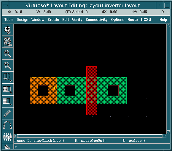
With this the nmos is complete, we can do the pmos. The pmos is drawn in the same fashion except that nactive becomes pactive and viceversa and nselect becomes pselect and viceversa. Also the width is twice larger and we need two contacts on each side. Notice that we have drawn the nmos with the active area 6 lambda below the Y: 0.00 axis, draw the pmos 6 lambda above the Y: 0.00 axis. You can use copy, stretch instead of drawing some of the shapes to make the layout faster. In the end you should get something like this:

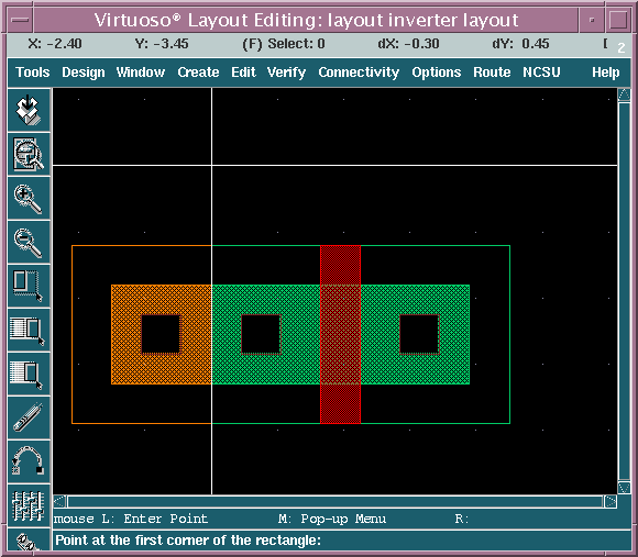
There is just one more element needed for the transistors: the nwell for the pmos. Draw a rectangle that surrounds the pmos active area by 6 lambda (1.8 microns), you should get:
We also need to add metal 1 above the contacts that needs to overlap the contacts by 1 lambda.

It is now time to save your design (Design -> Save) and run a preliminary DRC. Go to Verify -> DRC...
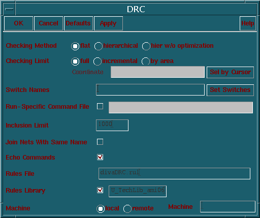
then click on OK. Check your CIW window, you should have no errors, in case you have errors you need to go back and fix them.
We are still not done with this lab yet! Until now we did what is
usually called

Now draw another path centered around the 0 axis to the end of the nwell.

Now let's connect the input. Draw a poly path between the two gates. Observe that the default width of the poly line is correct: 2 lambda.
Now start another poly line centered around the 0 axis going to the left and after you pass the 0,0 point and change to metal 1 by using the Change to Layer in the Create Path window. This should automatically insert a contact between poly and metal 1, click once to place the contact structure adjacent to the 0,0 point to the right. Double click when you reach the left-most edge of the nwell to end the path. In order to see all the layers in the contact "pcell" type Shift-F with the cursor in the layout window.
The only items left now are the vdd and gnd connections, we are going to use Create -> Polygon for those (we could also use rectangles or paths). Create the polygon using the points:
X: -1.35 Y: 4.65
X: -1.35 Y: 5.55
X: -3.30 Y: 5.55
X: -3.30 Y: 7.35
X: 5.70 Y: 7.35
X: 5.70 Y: 5.55
X: 1.35 Y: 5.55
X: 1.35 Y: 4.65
Again observe that except for a few of the points you don't really need to
look for the actual coordinates since they align with existing structures
(e.g. well or metal 1). The only sizes that you have to worry about are the
distance to other metal 1 (e.g. drain) which needs to be >3 lambda
and width of the line which we decided to be 6 lambda.
For the ground we will simply copy this polygon, go to Edit -> Copy and then click on Upside Down in the Copy window.
Now place the copied polygon at the bottom making conatct with the nmos source.

Save and run another DRC and make sure you have no errors. Congratulations, this is the end of Tutorial 5.