
. cdscdk2003 . cdscdk . cd cadence
Before you start Cadence this time you will need to copy a new configuration file (.simrc) used by LVS in your cadence directory. You only need to do that once. Type:
cp /net/cadence2001/download/ncsu-cdk/local/.simrc . icfb &
In this Tutorial 6 we are going to extract the layout of the inverter created in Tutorial 5, verify that the layout corresponds to the schematic (LVS) and simulate the extracted view with the extra parasitics.

Then observe that there are many instances where we have polygons and paths that abut each other to make a connection (e.g. metal 1 to metal 1, poly to poly, etc.). This is perfectly OK but takes more memory than if we "merge" them. In order to do that go to Edit -> Merge and then click on polygons and paths that can be merged (e.g. start with the output paths, then you can merge the vdd and gnd). Notice how they all become as if we had drawn polygons and there are no "lines" artificially separating the regions.
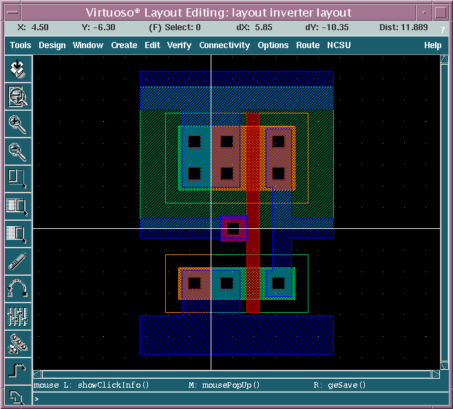
With this the cleanup is done and we can start preparing for extraction and LVS. In order to be able to do that we have to define the input and power supply pins in our layout as in the schematic. Go to Create -> Pin and enter IN as Name, input as I/O type and metal1 as Pin type.

Place the pin on the leftmost side of the metal 1 shape used as an input. Simlarly place an output pin OUT on the right most end of the output metal 1 polygon and two inputOutput pins called vdd! and gnd! for power and ground on the respective metal shapes on the top and bottom of the layout. Notice the 4 squares that represent the pins in the layout.

Go to Verify -> DRC... and make sure you have no design rules errors. No we can finally extract the layout. Go to Verify -> Extract... Click on Set Switches in the pop-up window and then choose Extract_parasitic_caps.

Notice that here you could have generated pselect and nselect layers automatically, you may decide to do that in the future to save effort. Now click on OK

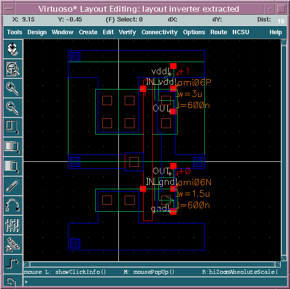
In the icfb window make sure you have no errors. If there are no errors you can now open the newly created extracted view from the Library Manager by double clicking. Press Shift-F to see the symbols for the extracted transistors. Notice that the extracted view is a layout that also has an underlying schematic.
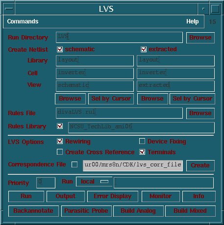
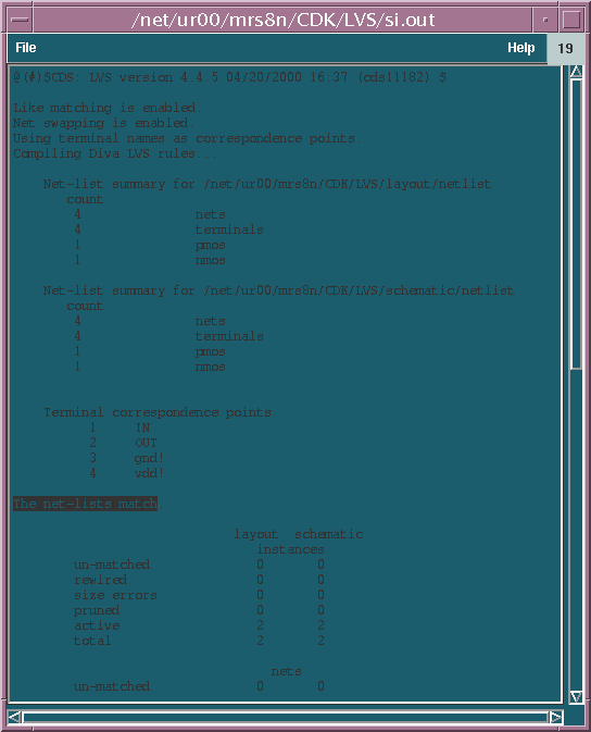
Press on Run and wait until the stop window pops up. This window simply signifies that LVS has terminated, not that the comparison was succesful. Click OK. In order to see that LVS verified the layout to correspond to the schematic click on Info in the LVS window.
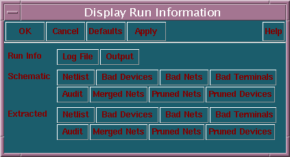
Now we can finaly verify. Click on Output and check to see that "The net-lists match" statement is made.
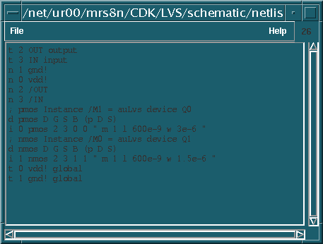
If you are curious you can also click on Netlist for the schematic and/or extracted and see how those look like.
First you need to create a symbol for your cell, in case you don't already have one, with Design -> Create Cellview -> From Cellview in the Composer window (from the original schematic). Then create a new cell schematic that you can call "testbench" that contains only your cell (as a symbol) with input and output ports and supply symbols (vdd and gnd). vdd and gnd need only be placed at the top level, no need to connect them to anything else.
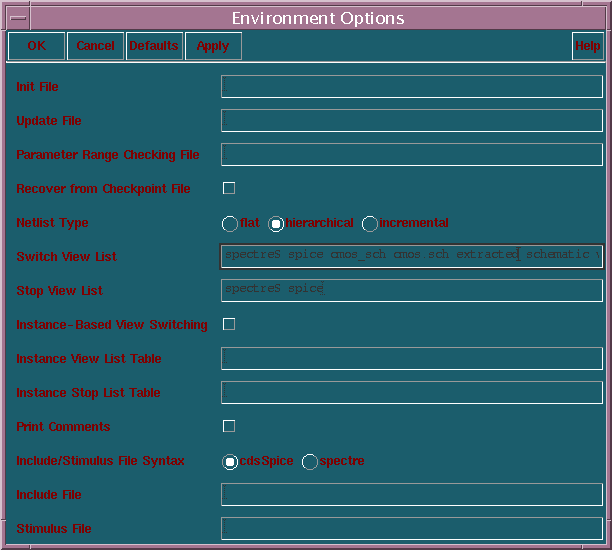
Now let's start Analog Artist, in the newly created "testbench" cell window go to Tools -> Analog Environment, then in the Analog Environment window go to Setup -> Environment. The line that we need to change is called the Switch View List. This entry is an ordered list of cell views that contain information that can be simulated. The simulator (in fact the netlister) will search until it finds one of these cellviews. The default entry does not contain an extracted cellview. We need to add an entry for extracted cellview in front of the schematic cellview. As a result of this modification, the simulator will use the extracted cell view of the cell, if one is available. Click OK.
Now you can continue exactly as in the simulation tutorial and the only difference will be that you are simulating the extracted view (with the parasitics) and not the schematic view. Congratulations, this is the end of Tutorial 6.