. cadence cd cadence icfb &
For more information on the various Cadence tools I encourage you again to read the corresponding user manuals. You can open the on-line manuals by typing:
openbook &
You can also get to the manuals by pressing the Help button on any Cadence window (e.g. CIW). Spend some time browsing the manuals to understand what is available. During the semester you will have to look for information in the on-line manuals to complement the (limited) info given by the tutorials.
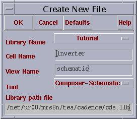
Now start the Library Manager by going to Tools -> Library Manager on the Tools menu of the CIW. Now the Tutorial library that you created previously should still appear in the Library Manager window. You can still use the same library for now. Let's start our second schematic now!
You should get the Composer schematic capture window. Spend some time analyzing the window. On the left side you have various shortcuts to common used commands such as: placing component instances (looks like an IC), drawing wires, placing ports, stretching, copying, zooming in and out, saving, etc. You also have access to these commands (and others) from the menu. It is not possible here to describe all the functionality of Composer so you are strongly encouraged to read the on-line user manual in openbook.
Let's start our second schematic which will be used to simulate a
simple CMOS inverter.
ATTENTION: The different screen capture files for this tutorial
are from an older tutorial using another technology, please make
sure you fill the values as in the text, not as in the screen shots!
Use what you learned in Tutorial 1 to capture the following schematic.
The big difference from Tutorial 1 is that we are no longer using
explicit power supplies. We are going to use input, output and
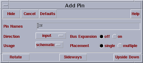
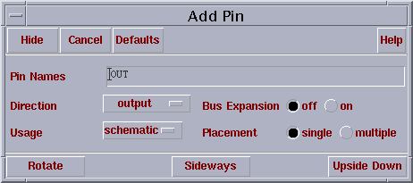
bidirectional ports instead. You can place these either by pressing the
PIN button on the left or by going to Add -> Pin... First
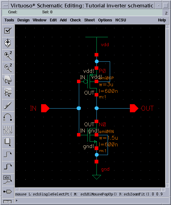
add one nmos4 transistor and one pmos4 transistor (from the
analogLib library), a gnd and a vdd symbol (from the basic library)
and then an input port IN and and output port OUT. Make sure you
choose input for IN:
and output for OUT:
Now connect everything with wires as an inverter and change the
transistor properties (see Tutorial 1) such that the nmos is 100n in
length and 300n in width and the pmos is 100n in length and 600n in
width. Also
specify a source and drain length for both transistors, let's make
them 300n.
Fill in nrvli (nMOS, regular Vthreshold, low leakage current)
as model name for the nmos and
prvli (pMOS, regular Vthreshold, low leakage current) as model
name for the pmos.
ATTENTION: The different screen capture files for this tutorial
are from an older tutorial using another technology, please make
sure you fill the values as in the text, not as in the screen shots!
Your final schematic should look like this:
Check and save and make sure you don't get any errors or warnings. Assuming there are no errors we are now ready to start simulation!
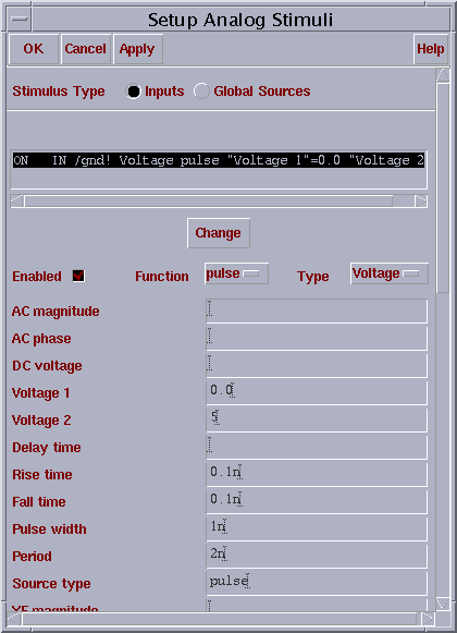
We also need to set up inputs and power supply since we don't have explicit voltage sources as in Lab1. Go to Setup -> Stimuli. Initially you have the Inputs chosen, you should have only one (IN). Click on Enabled, Function pulse, Type Voltage, Voltage1 0, Voltage2 1.5, Rise time 0.1n, Fall time 0.1n, Pulse width 1n, Period 2n, Source type pulse, and click on Apply. The input should turn from OFF to ON. CAUTION Cadence is very fragile concerning this dialog box, make srue you enter the numbers exactly as above (i.e. no space between the digit and n, etc.). If you get syntax errors later in siumlation they are most likely because of this.
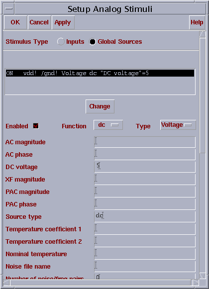
Now we need to setup the global sources (power supply). Click on the Global Sources, you should have only one (vdd!). Click on Enabled, Function dc, Type Voltage, DC voltage 1.5, Source type dc, and click on Apply. The vdd! should turn from OFF to ON.
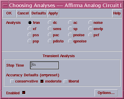
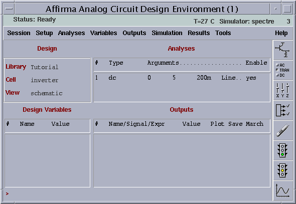
Now you need to choose the type of simulation, go to Analyses -> Choose... In this case we will choose tran which is the default, 4n as the Stop time (2 periods) and moderate as the accuracy default.
Now go to Outputs -> Save All and click on allpub for signals to save (default) and all for device currents. Click OK. CAUTION In general, once you have a big schematic, you will want to only save a few signals for simulation, this will make your simulation faster. For small circuits as we have now it doesn't make a big difference though.
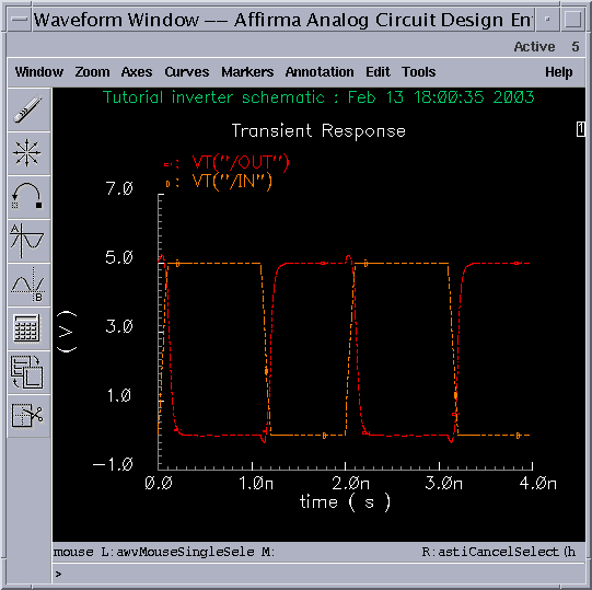
Now we can finally simulate! Click on the Netlist and Run button (looks like a green light) on the right or go to Simulation -> Netlist and Run. Click OK on the Welcome to Spectre window which should start the simulation. In case you have errors you will need to go back and correct them. This can be tricky! You may need to do Simulation -> Netlist -> Recreate if you change the schematic. CAUTION Each time you change the schematic you have to do Check and Save!. Assuming there are no errors you can now admire the simulation results. Go to Results -> Direct Plot -> Transient Signal which will pop-up your schematic window. Now you have to click on the signals you want to see. Since this is a transient analysis we want to see the input and output voltages. In order to do this you have to click on the input and output nets, then the ESC key. You should finally get the desired simulation results, 2 glorious periodic signals as expected from an inverter.
We are now almost done, before we finish let's try to also plot the VTC for the inverter. For this we first need to replace the IN pin by another vdc power supply from the analogLib library as in Tutorial 1. Change its DC voltage property to 1.5

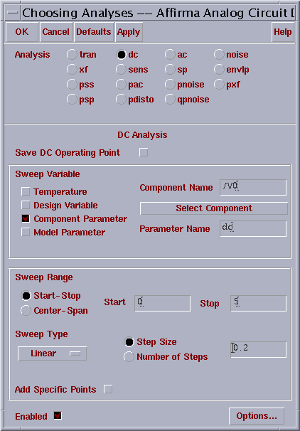
Check and Save (make sure you get no errors). Now go to Analyses -> Choose, dc and Component Parameter, Select Component (as in Lab1), then the voltage source in the schematic, then choose 0 as Start, 1.5 as Stop and 0.1 as step.
Now click on the old tran analysis and then go to Analyses -> Delete so that you are left with only one Analysis.
Finally do Netlist and Run. If you don't have any errors
you can now go to Results -> Direct Plot -> DC and click
on the output net and the ESC key to get a glorious inverter VTC as in the
textbook.
ATTENTION: The different screen capture files for this tutorial
are from an older tutorial using another technology, please make
sure you fill the values as in the text, not as in the screen shots!

It is a good idea to save your state before exiting the simulator in case you want to redo some of the simulations you can start by loading a saved state. Congratulations, this is the end of Tutorial 2.